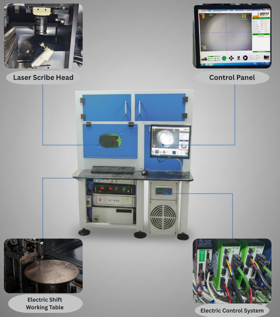
SLDM 200 Laser Wafer Dicing Machine
Semiconductor Manufacturing Equipment
SLDM-200 Laser Wafer Dicing Machine
High Precision Semi-Automatic Laser Wafer Dicing System for Silicon, Glass, Sapphire, MEMS and Semiconductor Applications up to 200mm Wafer Size.
Wafer Size
Up to 200 mm
Thickness
10µm – 200µm
Laser
532nm Green
Warranty
3 Years
✓ Semiconductor Grade Precision
✓ Green Laser Technology
✓ Industrial Motion Control
✓ 3-Year Warranty
What is the SLDM-200 Laser Wafer Dicing Machine?
The SLDM-200 Laser Wafer Dicing Machine is a high-precision semi-automatic wafer processing system designed for semiconductor manufacturing, MEMS production, sensor fabrication and advanced electronics applications. Using a 532nm pulsed green laser, the machine delivers accurate wafer singulation with reduced mechanical stress, minimal chipping and superior edge quality.
Product Overview
Semiconductor Wafer Dicing With Exceptional Precision
Designed for modern semiconductor manufacturing environments, the SLDM-200 combines precision optics, advanced motion control and industrial automation into a compact platform capable of processing silicon, glass, sapphire and specialty wafers.
High Precision Laser Processing
Narrow beam diameter of 10–20µm enables highly accurate wafer separation while minimizing heat affected zones and reducing micro-crack formation.
Semiconductor Manufacturing Ready
Designed specifically for wafer-level manufacturing processes where dimensional accuracy, repeatability and process stability are critical.
Supports Multiple Materials
Process silicon wafers, glass wafers, sapphire substrates, MEMS wafers, ceramic substrates and specialty semiconductor materials.
Industrial Reliability
Industrial control architecture ensures consistent production performance, reduced downtime and reliable operation under demanding manufacturing conditions.
Technical Highlights
Key Technical Parameters
Laser Type
Pulsed Green Laser
Wavelength
532nm
Beam Size
10–20µm
Operation
Semi Automatic
Wafer Diameter
Up to 200mm
Thickness Range
10µm–200µm
SLDM-200 Laser Wafer Dicing Machine
Discuss Your Application Requirement
WhatsApp Inquiry
Key Features
Engineered For Precision Semiconductor Manufacturing
The SLDM-200 combines precision laser technology, industrial automation, and semiconductor-grade motion control to achieve reliable wafer singulation with superior edge quality.
532nm Green Laser Source
Optimized wavelength for high absorption in semiconductor materials, enabling clean and controlled wafer processing.
Ultra Fine Beam Diameter
Beam size of 10–20µm enables narrow kerf cutting and exceptional dimensional accuracy.
200mm Wafer Support
Supports semiconductor wafers up to 200mm diameter for a wide range of production applications.
Precision Servo Motion
High accuracy positioning system ensures repeatable processing and consistent quality.
Industrial HMI Control
User-friendly touchscreen interface enables fast setup and process management.
Low Stress Processing
Minimizes mechanical stress compared to conventional blade dicing methods.
Technical Specifications
SLDM-200 Technical Data Sheet
| Parameter | Specification |
|---|---|
| Model Number | SLDM-200 |
| Machine Type | Laser Wafer Dicing Machine |
| Operation Mode | Semi Automatic |
| Application | Semiconductor Wafer Dicing |
| Supported Wafer Size | Up to 200 mm |
| Wafer Thickness Range | 10 µm – 200 µm |
| Laser Type | Pulsed Green Laser |
| Laser Wavelength | 532 nm |
| Beam Size | 10 – 20 µm |
| Motion Control | Precision Servo System |
| Control Interface | Industrial HMI Touchscreen |
| Warranty | 3 Years |
Advantages
Benefits Beyond Conventional Dicing Technologies
Reduced Chipping
Laser processing significantly reduces edge chipping, improving final die quality.
Narrow Kerf Width
Maximizes wafer utilization and increases production yield.
Minimal Mechanical Load
Eliminates blade contact and reduces wafer damage risk.
Superior Accuracy
Ideal for advanced semiconductor devices requiring micron-level precision.
Lower Maintenance
No blade wear issues commonly associated with mechanical dicing systems.
Higher Yield
Improved cutting quality contributes directly to manufacturing efficiency.
Applications & Industries
Suitable For Diverse High-Tech Manufacturing Sectors
| Industry | Application | Benefits |
|---|---|---|
| Semiconductor Manufacturing | Wafer Singulation | High Accuracy & Yield |
| MEMS Manufacturing | Sensor Wafer Dicing | Reduced Mechanical Stress |
| LED Industry | Sapphire Wafer Processing | Clean Edge Quality |
| Power Electronics | Device Separation | Precision Cutting |
| Research Institutions | Prototype Development | Flexible Process Capability |
| Microelectronics | Advanced Packaging | Improved Reliability |
Material Compatibility
Process A Wide Range Of Semiconductor Materials
| Material | Thickness Range | Processing Method | Typical Industry |
|---|---|---|---|
| Silicon Wafer | 10–200µm | Laser Dicing | Semiconductors |
| Glass Wafer | 30–200µm | Laser Cutting | MEMS & Sensors |
| Sapphire Wafer | 50–150µm | Laser Dicing | LED Manufacturing |
| Ceramic Substrate | 50–200µm | Precision Cutting | Electronics |
| MEMS Wafer | 20–150µm | Micro Dicing | Sensor Manufacturing |
| Compound Semiconductor | 20–150µm | Laser Processing | Photonics & RF |
Need Material Feasibility Testing?
Share your wafer material, thickness and application details with our engineering team.
Discuss Your Application
Machine Capabilities
Designed For Advanced Semiconductor Manufacturing Requirements
The SLDM-200 Laser Wafer Dicing Machine combines high-precision motion control, semiconductor-grade optics, and advanced laser processing technology to deliver repeatable, high-quality wafer singulation.
200mm Wafer Processing
Supports wafer diameters up to 200mm for semiconductor, MEMS and sensor manufacturing applications.
Ultra-Thin Wafer Handling
Processes wafers as thin as 10µm with high stability and precision.
Micro Precision Dicing
Fine laser spot size enables micron-level processing accuracy.
High Repeatability
Precision servo system ensures consistent production quality.
Complex Pattern Processing
Suitable for intricate semiconductor layouts and advanced packaging applications.
Low Thermal Impact
Optimized laser parameters minimize damage to surrounding structures.
Working Principle
How The SLDM-200 Laser Wafer Dicing Process Works
01
Wafer Loading
The wafer is securely mounted onto the precision worktable.
02
Vision Alignment
Fiducial marks and cutting paths are aligned using precision positioning.
03
Laser Scribing
The 532nm pulsed laser creates highly accurate separation paths.
04
Wafer Separation
Individual dies are separated with excellent edge quality and minimal defects.
Why Choose SLDM-200
Built For Precision, Reliability And Production Efficiency
Semiconductor Focused Design
Developed specifically for wafer dicing and microelectronics manufacturing.
Reduced Chipping
Achieves cleaner wafer edges compared to conventional mechanical methods.
Higher Production Yield
Lower defect rates contribute to improved manufacturing efficiency.
Industrial Automation
Reliable motion control system designed for long operating cycles.
Flexible Material Compatibility
Supports silicon, glass, sapphire and advanced semiconductor materials.
3-Year Warranty
Long-term support and confidence for industrial users.
Technology Comparison
Laser Dicing Vs Conventional Blade Dicing
| Parameter | SLDM-200 Laser Dicing | Blade Dicing |
|---|---|---|
| Mechanical Stress | Very Low | High |
| Chipping Risk | Minimal | Moderate to High |
| Tool Wear | No Blade Wear | Regular Blade Replacement |
| Precision | Excellent | Good |
| Maintenance Cost | Lower | Higher |
| Yield | Higher | Lower |
ROI Benefits
Improve Manufacturing Economics
Higher Yield
Reduced wafer damage increases usable die output.
Lower Consumable Cost
Eliminates frequent blade replacement expenses.
Reduced Rework
Consistent cutting quality minimizes downstream defects.
Reduced Downtime
Stable laser operation improves machine availability.
Productivity Benefits
Faster And More Consistent Production
Reduced Setup Time
User-friendly control interface accelerates process preparation.
Consistent Accuracy
Stable process parameters reduce operator dependency.
Continuous Operation
Industrial components support extended production schedules.
Efficient Material Utilization
Narrow kerf width increases wafer utilization.
Quality Benefits
Superior Semiconductor Manufacturing Quality
Clean Cut Edges
Produces high-quality separation with reduced edge damage.
Improved Yield
Better die quality results in fewer rejected components.
Reduced Cracking
Lower mechanical force minimizes micro-crack formation.
Repeatable Results
Consistent process performance across production batches.
Safety Benefits
Industrial Safety Designed Into Every System
Enclosed Processing Area
Helps maintain safe laser operation during processing.
Industrial Control System
Reliable machine operation with integrated safety functions.
Stable Motion Platform
Precision movement improves process consistency and safety.
Operator-Friendly Interface
Simplifies machine operation and monitoring.
Installation Requirements
Facility Preparation Guidelines
Proper installation conditions ensure maximum machine performance, process stability and long-term reliability.
| Requirement | Recommended Specification |
|---|---|
| Power Supply | Industrial Power Source |
| Compressed Air | Clean & Dry Air Supply |
| Operating Environment | Dust Controlled Area |
| Floor Condition | Level Industrial Floor |
| Machine Clearance | Minimum 1 Meter Around Machine |
| Operator Access | Front Side Accessibility |
Maintenance Information
Keep Your Production Running Efficiently
Daily Inspection
Verify laser optics cleanliness, worktable condition and system status before operation.
Weekly Maintenance
Check motion system, alignment accuracy and machine cleanliness.
Monthly Inspection
Review laser performance, cooling system operation and positioning repeatability.
Preventive Service
Scheduled servicing helps reduce unexpected downtime and maintain process quality.
Troubleshooting Insights
Common Processing Considerations
| Observation | Possible Cause | Recommended Action |
|---|---|---|
| Inconsistent Cut Quality | Parameter Mismatch | Review Process Settings |
| Position Error | Alignment Deviation | Perform Calibration Check |
| Reduced Processing Efficiency | Optics Contamination | Inspect Optical Components |
| Irregular Edge Finish | Material Variation | Optimize Processing Parameters |
Expert Summary
Why Manufacturers Choose The SLDM-200
The SLDM-200 Laser Wafer Dicing Machine is engineered for precision semiconductor manufacturing where yield, accuracy and process reliability directly impact production profitability. The combination of a 532nm pulsed laser source, ultra-fine beam diameter and precision motion control enables efficient wafer singulation across silicon, glass, sapphire and advanced semiconductor materials.
What is a Laser Wafer Dicing Machine?
A laser wafer dicing machine is a precision semiconductor manufacturing system used to separate wafers into individual dies using highly focused laser energy.
What Materials Can SLDM-200 Process?
Silicon wafers, glass wafers, sapphire wafers, MEMS substrates, ceramic substrates and advanced semiconductor materials.
What Industries Use This Machine?
Semiconductor manufacturing, MEMS production, sensor fabrication, LED manufacturing, photonics and advanced electronics industries.
Why Choose Laser Dicing?
Laser dicing reduces chipping, minimizes mechanical stress, improves yield and provides superior precision compared to conventional blade dicing.
Frequently Asked Questions
Technical Questions About SLDM-200
The SLDM-200 supports wafer diameters up to 200mm.
The machine supports wafer thicknesses from 10µm to 200µm.
A high precision 532nm pulsed green laser system.
Yes, Sigma Laser Technologies provides installation assistance, training and after-sales support.
The machine is supplied with a 3-Year Warranty.
Discuss Your Application
Looking For A Wafer Dicing Solution?
Connect directly with Sigma Laser Technologies to discuss your wafer material, thickness, production requirements and process objectives.